20+ fir filter block diagram
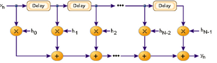
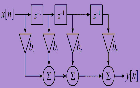
A sample delay line and a set of coefficients. The terms represent unit delays.

Rf Canceller Analog Fir Filter Block Diagram Download Scientific Diagram
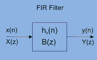
A finite impulse response FIR filter is a filter structure that can be used to implement almost any sort of frequency response digitally.
. In the digital signal processing system the use of FIR short form is one type of filter whose impulse response is of finite duration the reason of it settles zero in finite. Basic IIR Digital Filter Structures 1. The number of stages of an FIR filter to be designed will also depend on the order of the filter.
The Lattice Serial FIR filter uses serial arithmetic elements to achieve a compact size. Of the above FIR filter is. Finite Impulse Response.
Structurally FIR filters consist of just two things. Computer Science questions and answers. Therefore the half and the full adder are used to construct the 4-bit binary adder.
5120 Draw the block diagram in the direct form for the FIR filter when the frequency response is given by. Due to the serial nature of the arithmetic the data rate is slower than the clock rate and dependant on the. Multiply each sample in the delay.
The shaping filter is based on a direct FIR but what makes it different is the delay line instead of having one delay. Put the input sample into the delay line. Block diagram of an Interpolated FIR filter.
The block diagram shown in the following figure serves as a foundation for particular adaptive filter realisations such as Least Mean Squares LMS and Recursive Least Squares RLS. If the order of the filter is N then the number of stages to be used in the filter. Note that while this representation for a delay element is common and widely accepted in the signal processing community the specification of delay in.
An FIR filter is. To implement the filter. 5120 Draw the block diagram in the direct form for the FIR.
The 4-bit adder performs computing function of the FIR filter. FIR filter block diagram. Block Diagram Representation Input-output relation of an LTI system can be realized using different computational algorithms.
Draw the block diagram of 3rd order FIR filter. The proposed half adder is. Write the difference equation for the filter and find out the.
What Is Fir Filter Fir Filters For Digital Signal Processing

7 Block Diagram Of A 4 Tap Fir Filter Download Scientific Diagram

Fir Filter Block Diagram Download Scientific Diagram

Schematic Diagram Of The Fir Filter Download Scientific Diagram
Block Diagram Of Fir Filter Coefficient Calculation Algorithm Download Scientific Diagram

Block Diagram Of The Fpga Based Fir Filter Download Scientific Diagram

The Proposed Structure Of The Da Based Fir Filter For Fpga Download Scientific Diagram
![]()
Structure Of Fir Filter A Transposed Form B Fir Filter Using A Download Scientific Diagram
What Is Fir Filter Fir Filters For Digital Signal Processing

Rtl Schematic Of Fir Filter Download Scientific Diagram

Block Diagram Of Digital Fir Filter 22 Download Scientific Diagram

9 Fir Filter Block Diagram Download Scientific Diagram
A Simple Data Flow Graph For A A Three Tap Fir Filter B A Download Scientific Diagram

Block Diagram Of The Fir Filter With Sdm Modulated Input Signal Download Scientific Diagram
What Is Fir Filter Fir Filters For Digital Signal Processing

Basic Block Diagram Of Fir Filter Download Scientific Diagram

3 Block Diagram Of A Fir Filter Download Scientific Diagram